More Post from the Author
- Huawei lanza el programa "AHEAD"
- Segway Powersports oivuje Quad Challenge na Red Bull Erzbergrodeo a podporuje rast eurpskej kultry pretekov tvorkoliek
- Bybit Launches IPO Express, Becoming One of First Centralized Crypto Exchanges to Offer Tokenized IPO Access, Starting With SpaceX
- Ramtech VP of Business Development Kelly Williams to Speak on Modular Construction Benefits in Panel Discussion at 2026 InterFace Houston Multifamily Conference
- CueCue Launches Interactive Web Card to Help People Earn From Skills, Services and Idle Assets
E&R: Taiwan's Leading Semiconductor Equipment Supplier Driving Advanced Packaging Innovation
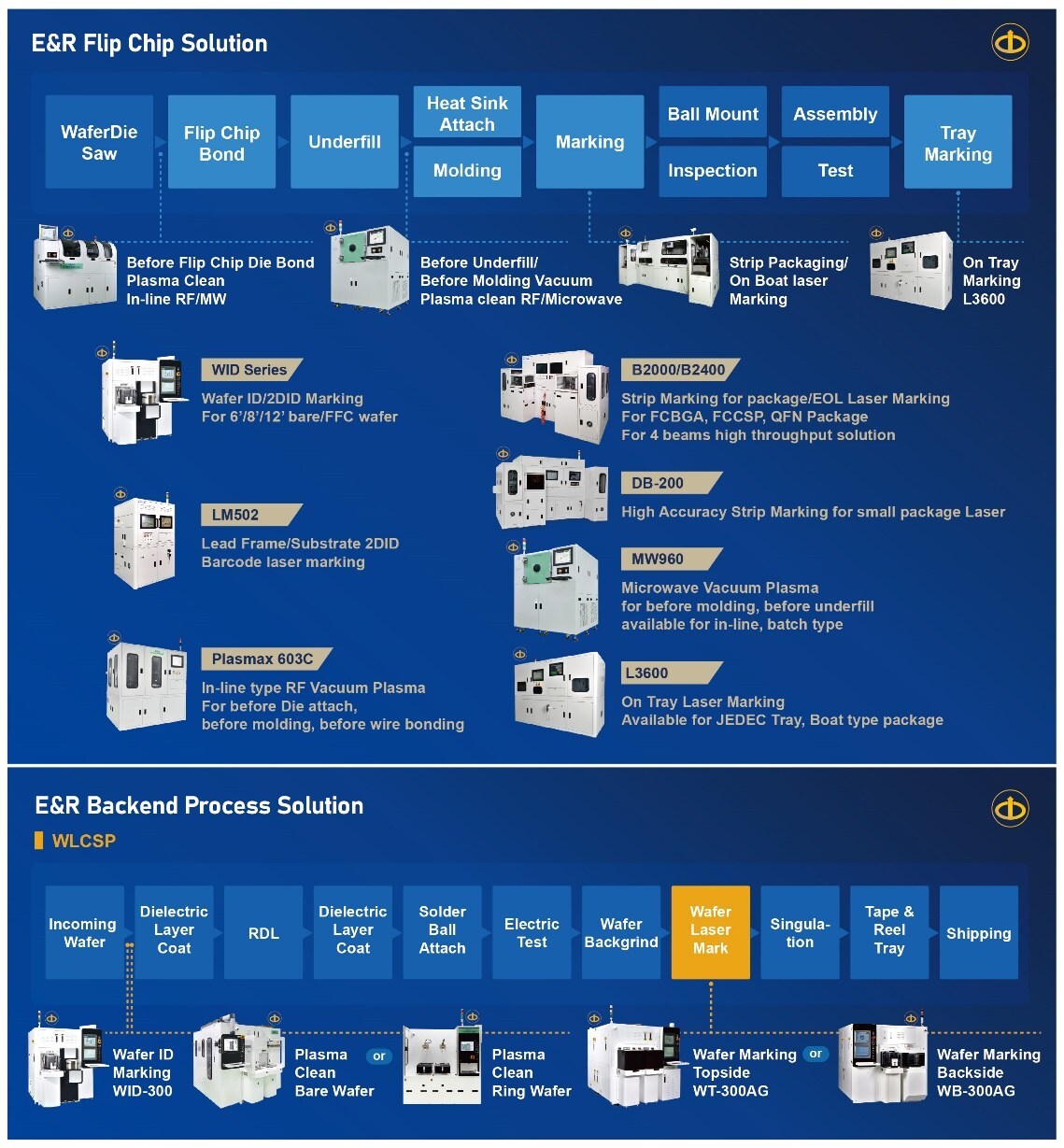
KAOHSIUNG, Feb. 12, 2025 /PRNewswire/ -- E&R (E&R Engineering Corp.), a Taiwan-based semiconductor equipment manufacturer with 30 years of expertise, has supplied over 500 advanced semiconductor packaging tools to majorOSATs worldwide, specializing in laser and plasma solutions. Its laser technologies include marking, scribing, grooving, and wafer ID/backside marking, while its vacuum plasma solutions enable surface cleaning, oxide removal, and pre-bonding/pre-underfill/ pre-molding treatment to enhance package reliability and yield.


Taiwan-Made Excellence with OSAT-Grade Precision
E&R ensures top-tier quality through MIT (Made in Taiwan) manufacturing, integrating key components from leading European and U.S. suppliers. All machines are manufactured, assembled, and tested in Taiwan, delivering high-performance solutions for advanced packaging platforms such as FCBGA, FCCSP, Fan-Out, and Fan-In (Wafer Level Packaging). Its Flip Chip BGA solutions include pre-flip chip die bond plasma cleaning, pre-molding/underfill plasma cleaning, and on boat/tray laser marking for traceability, ensuring high-quality, reliable packaging processes that meet the demands of modern semiconductor manufacturing.
FOPLP (Fan-Out Panel Level Packaging)
E&R provides reliable, mass-production equipment for FOPLP processes, supporting panel sizes from 300 300 mm to 700 700 mm. Its solutions encompass laser marking, laser cutting, plasma cleaning post-drilling, de-smear, laser debonding, post-debond plasma descum, and ABF drilling, all featuring excellent warpage handling capabilities of up to 16 mm to ensure high-efficiency output.
Strong Global Service Support
With service teams based in Portland, Arizona, and New Mexico, E&R delivers fast after-sales support to minimize downtime and maximize production efficiency. Its deep expertise in Advanced Packaging allows for quicker issue resolution and improved yields. Backed by comprehensive technical support, remote diagnostics, and customized training, E&R reinforces its reputation as a trusted partner for semiconductor manufacturers worldwide.
As demand for high-performance semiconductor packaging grows, E&R drives innovation in Advanced Packaging with high-precision laser and plasma solutions, enhancing efficiency, yield, and reliability for North American and European manufacturers while supporting localized supply chain resilience.
For more information, please visit: https://en.enr.com.tw/
Contact Information:[emailprotected]/ [emailprotected]
SOURCE E&R Engineering Corp

More Post from the Author
- Huawei lanza el programa "AHEAD"
- Segway Powersports oivuje Quad Challenge na Red Bull Erzbergrodeo a podporuje rast eurpskej kultry pretekov tvorkoliek
- Bybit Launches IPO Express, Becoming One of First Centralized Crypto Exchanges to Offer Tokenized IPO Access, Starting With SpaceX
- Ramtech VP of Business Development Kelly Williams to Speak on Modular Construction Benefits in Panel Discussion at 2026 InterFace Houston Multifamily Conference
- CueCue Launches Interactive Web Card to Help People Earn From Skills, Services and Idle Assets